

Oxide semiconductors typically show superior device performance compared to
amorphous silicon or organic counterparts, especially, when they are physical vapor deposited.
However, it is not easy to reproduce identical device characteristics when the oxide field-
effect transistors (FETs) are solution-processed/ printed; the level of complexity further
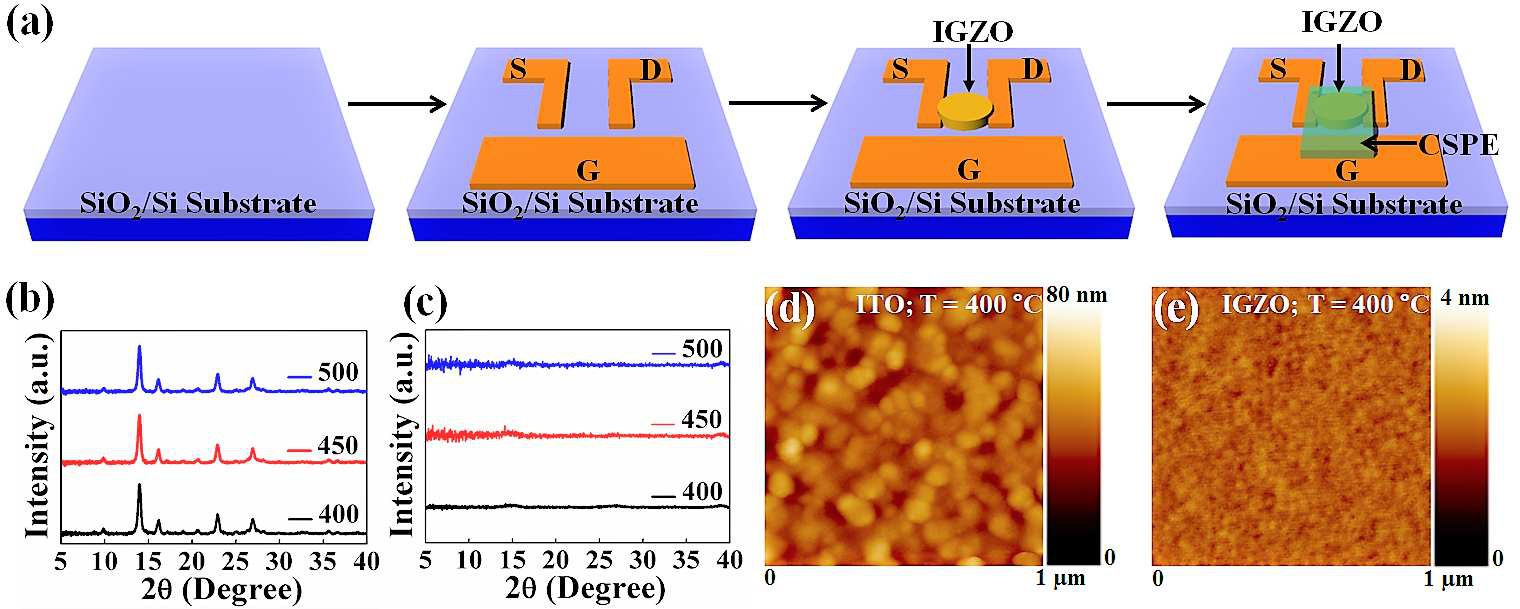
intensifies with the need to print the passive elements as well. Here, we developed a protocol
for designing the most electronically compatible electrode/ channel interface based on the
judicious material selection. Exploiting this newly developed fabrication schemes, we are now
able to demonstrate high-performance all-printed FETs and logic circuits using amorphous
indium-gallium-zinc oxide (a-IGZO) semiconductor, indium tin oxide (ITO) as electrodes and
composite solid polymer electrolyte as the gate insulator. Interestingly, all-printed FETs
demonstrate an optimal electrical performance in terms of threshold voltages and device
mobility and may very well be compared with devices fabricated using sputtered ITO
electrodes. This observation originates from the selection of electrode/ channel materials from
the same transparent semiconductor oxide family, resulting in the formation of In-Sn-Zn-O (ITZO) based diffused a-IGZO/ ITO interface that controls doping density while ensuring
high electrical performance. Compressive spectroscopic studies reveal that Sn doping
mediated excellent band alignment of IGZO with ITO electrodes is responsible for the
excellent device performance observed. All-printed n-MOS based logic circuits have also
been demonstrated towards new-generation portable electronics.