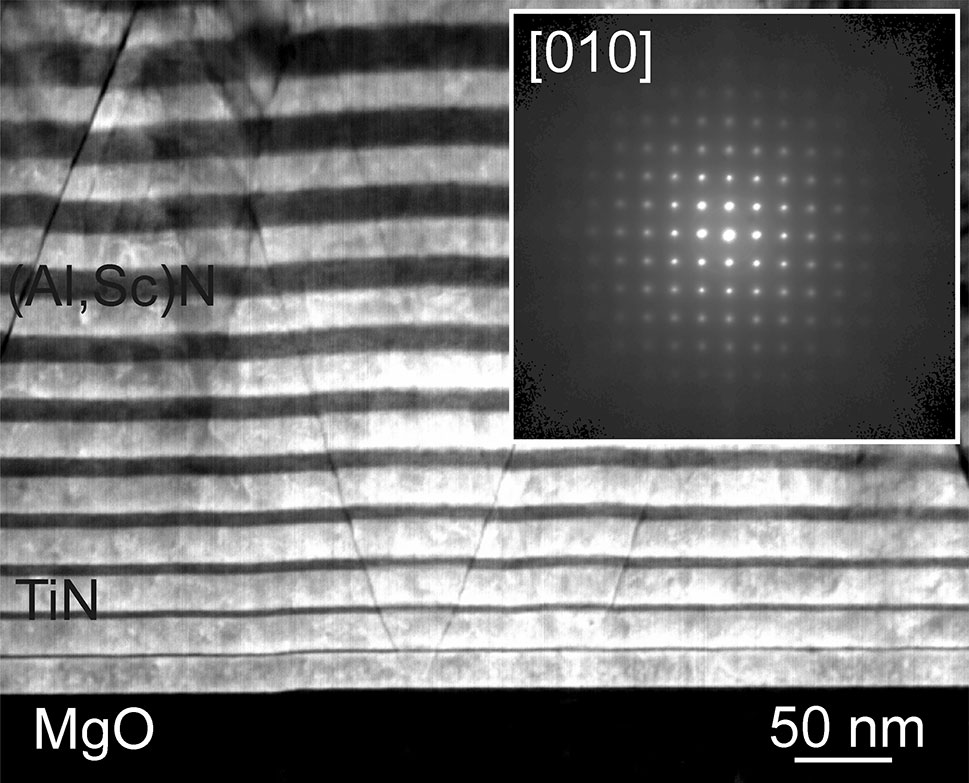
Alternative designs of plasmonic metamaterials for applications in solar energyharvesting devices are necessary due to pure noble metal-based nanostructures’ incompatibility with CMOS technology, limited thermal and chemical stability, and high losses in the visible spectrum. In the present study, we demonstrate the design of a material based on a multilayer architecture with systematically varying dielectric interlayer thicknesses that result in a continuous shift of surface plasmon energy. Plasmon resonance characteristics of metal/semiconductor TiN/(Al,Sc)N multilayer thin films with constant TiN and increasing (Al,Sc)N interlayer thicknesses were analyzed using aberration-corrected and monochromated scanning transmission electron microscopy-based electron energy loss spectroscopy (EELS). EEL spectrum images and line scans were systematically taken across layer interfaces and compared to spectra from the
centers of the respective adjacent TiN layer. While a constant value for the TiN bulk plasmon resonance of about 2.50 eV was found, the surface plasmon resonance energy was detected to continuously decrease with increasing (Al,Sc)N interlayer thickness until 2.16 eV is reached. This effect can be understood to be
the result of resonant coupling between the TiN bulk and surface plasmons across the dielectric interlayers at very low (Al,Sc)N thicknesses. That energy interval between bulk and decreasing surface plasmon resonances corresponds to wavelengths in the visible spectrum. This shows the potential of tailoring the
material’s plasmonic response by controlling the (Al,Sc)N interlayer thickness, making TiN-based ultilayers good prospects for plasmonic metamaterials in energy devices.


